Concept & Scope
A potentiometer-controlled LED brightness circuit seems straightforward, until you learn that LEDs should not be dimmed by varying voltage. The correct approach is pulse-width modulation: keeping voltage constant and varying the ratio of on-time to off-time. Any microcontroller can do this, but for a simple lamp, adding a microcontroller is unnecessary overhead.
The NE555 timer IC can generate a PWM signal in "astable" mode with no firmware required. A potentiometer adjusts the duty cycle directly, and the result is smooth, flicker-free dimming from a purely analog circuit.
Design Philosophy: Use the simplest technology that solves the problem. A NE555 costs less than a dollar and requires no programming, firmware, or debugging. For a lamp, it's the right tool for the job.
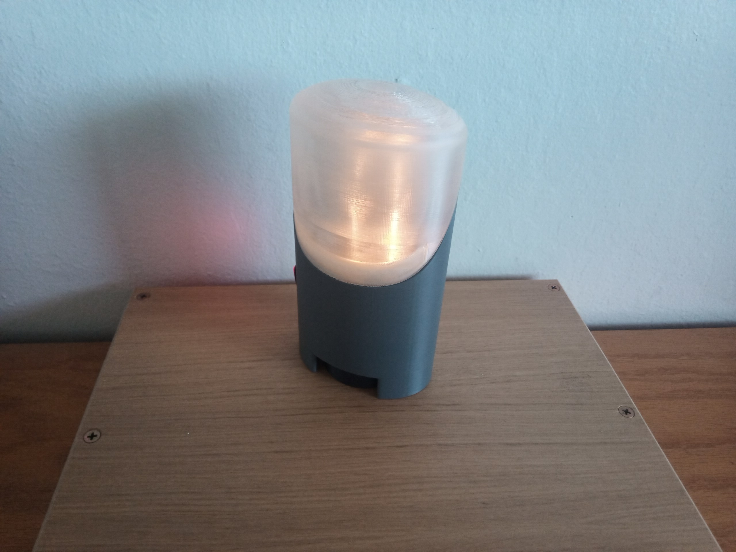
// The finished lamp.
Circuit Design
The circuit is built around a NE555 in an astable configuration. The potentiometer varies the time constants that govern the charge/discharge cycle, controlling duty cycle and thus perceived brightness. A pair of diodes steers current through the pot in one direction only, enabling a wide dimming range without the circuit locking up at the extremes. The reference below, and the inspiration for this project, came from The Big Book of Maker Skills, by Chris Hackett.
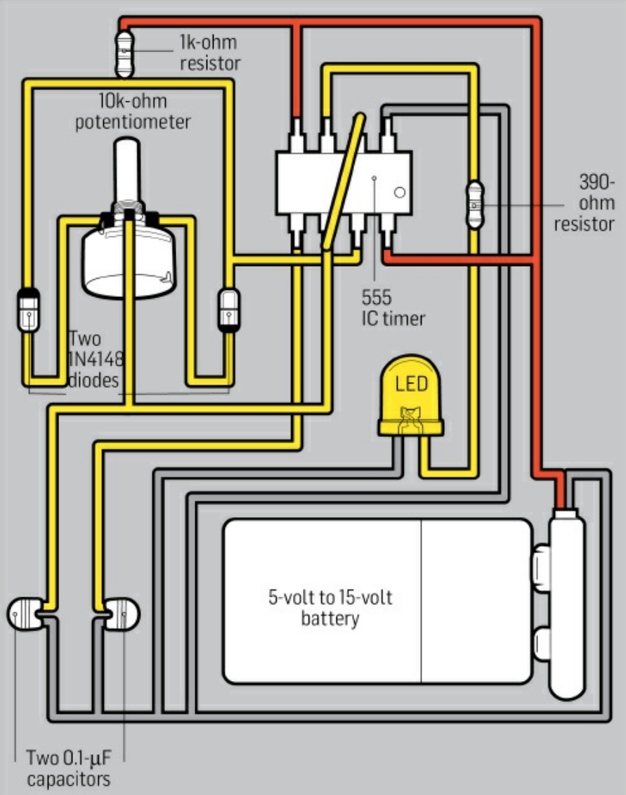
// Reference circuit diagram (NE555 astable PWM configuration). This schematic was the starting point before component selection and layout.
Simulation
Before ordering components, the circuit was modeled in Falstad — a browser-based circuit simulator — to visualize the waveform and verify the duty cycle range across the potentiometer sweep.
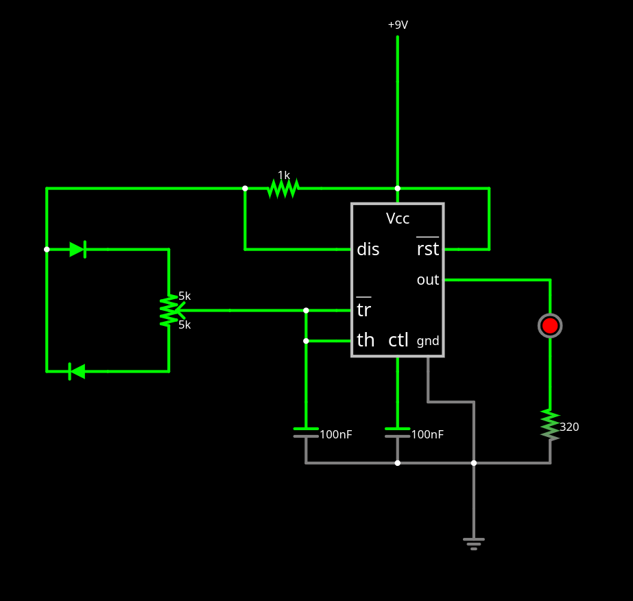
// Falstad simulation of the PWM circuit.
KiCAD — Schematic & Layout
With the circuit validated in simulation, components were selected and their exact footprints were either taken from the manufacturer, or derived manually. The schematic was drawn in KiCAD, then translated into a PCB layout sized to fit within the area of the PCB blank.
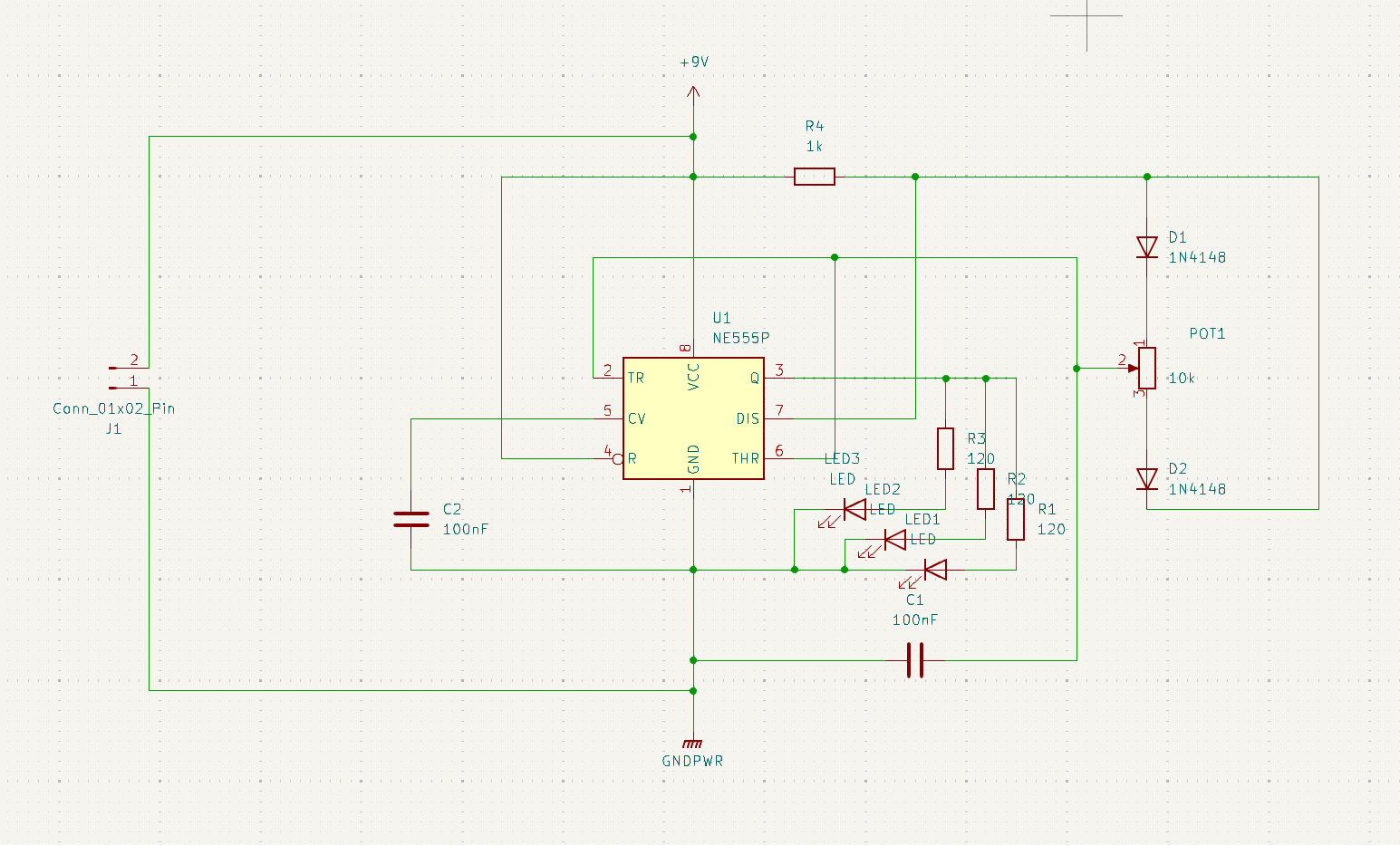
// KiCAD schematic
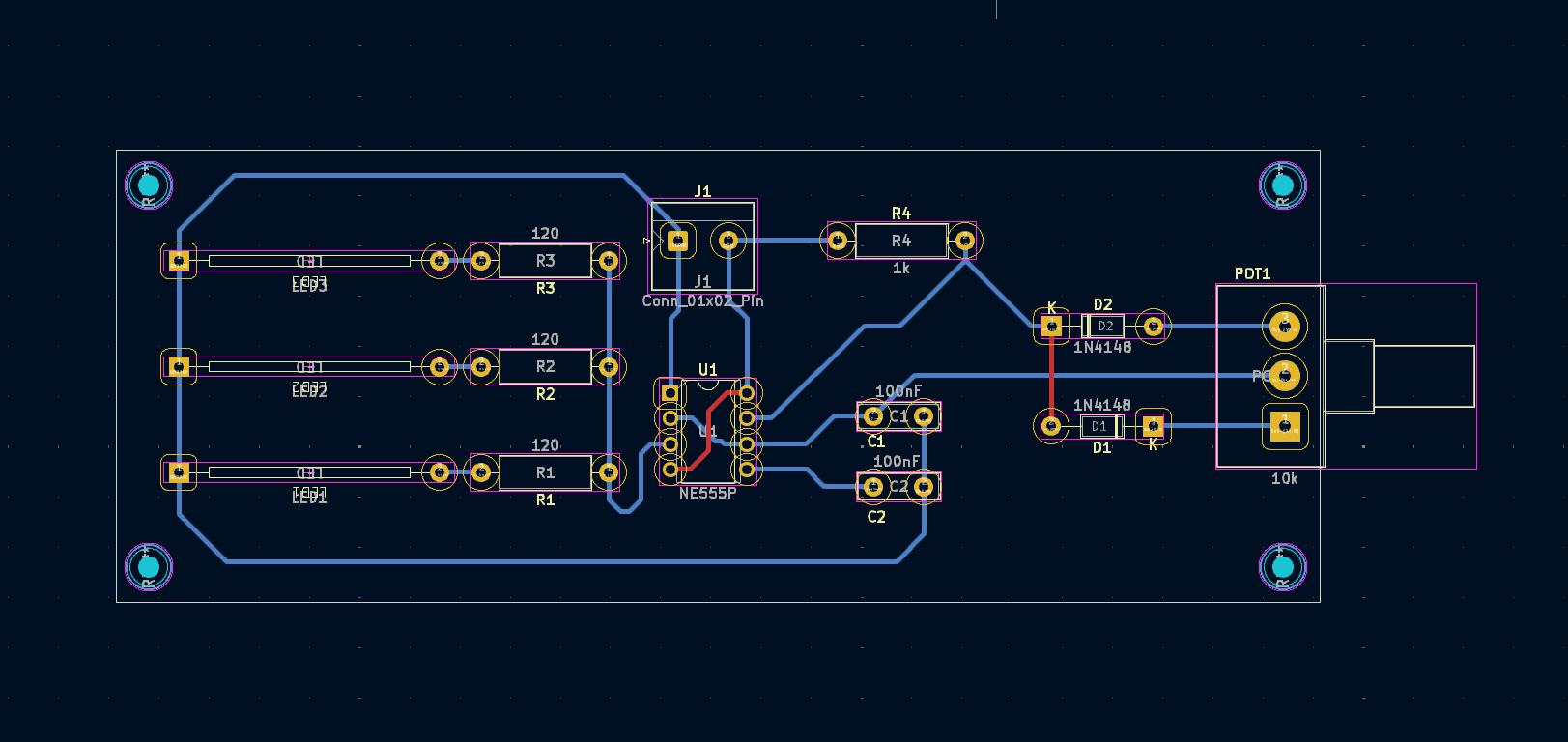
// KiCAD footprint layout — traces routed for double-sided milling. Component leads placed on the back side wherever possible to simplify milling.
Mill Tip: The CNC can mill only one side of a board per setup. If you must draw traces on both sides (to avoid crossing , you will have to locate your origin thoughtfully when setting up for milling.
Proof of Concept Sample
Before committing to a milled PCB, the circuit was assembled on a breadboard using pre-soldered components — a fast, cheap way to confirm that the NE555 configuration actually behaved as simulated. The breadboard sample verified the PWM signal and the full dimming range in hand before any fabrication work began.
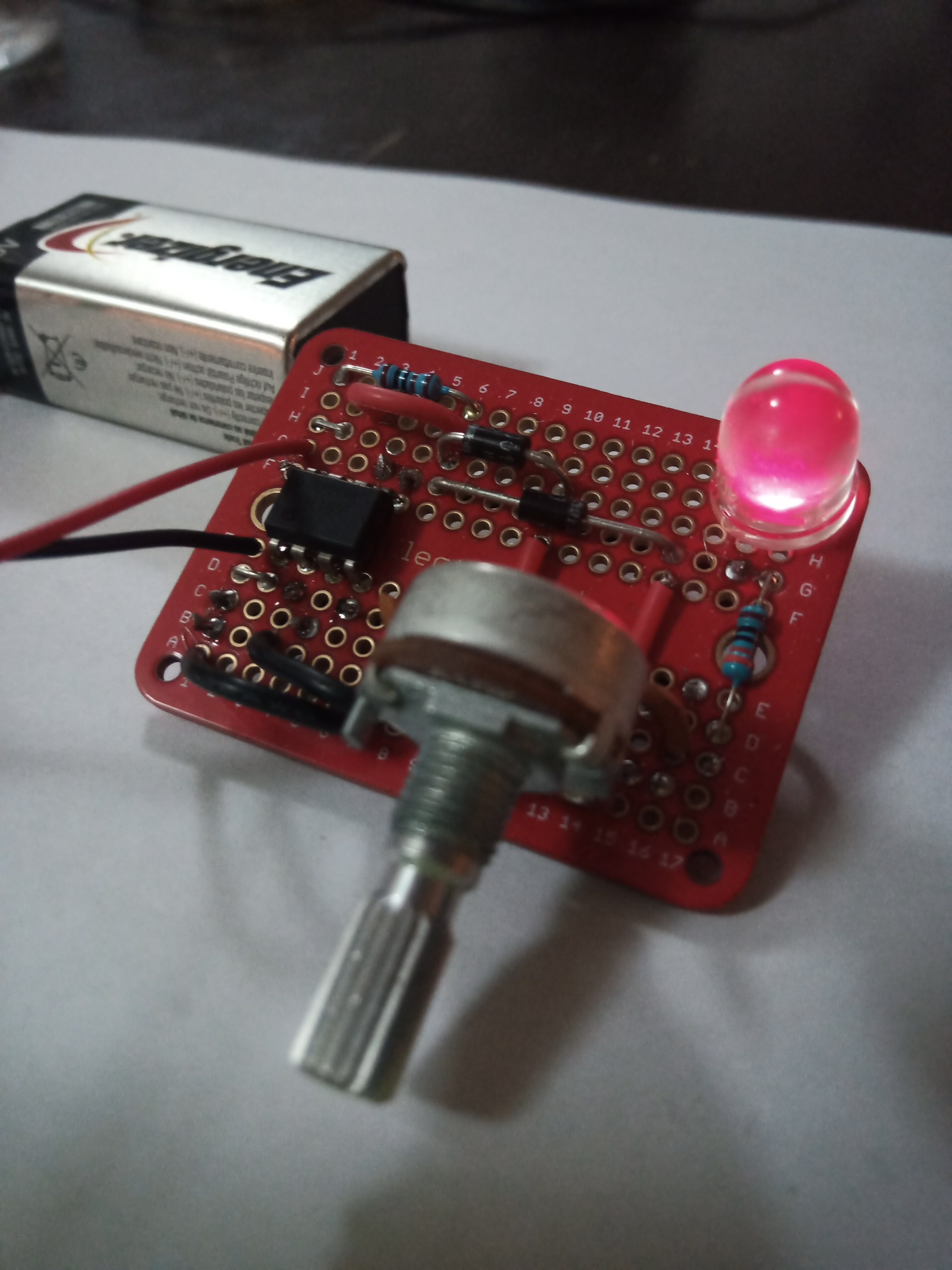
// Working proof-of-concept on a breadboard — circuit confirmed before committing to the final PCB.
PCB Fabrication
The board was milled out of an FR-1 blank, a flat panel of paper (basically cardstock) with a thin layer of copper bonded to each side. The machine cuts a series of loops and thru-holes, leaving traces in the "negative" space.
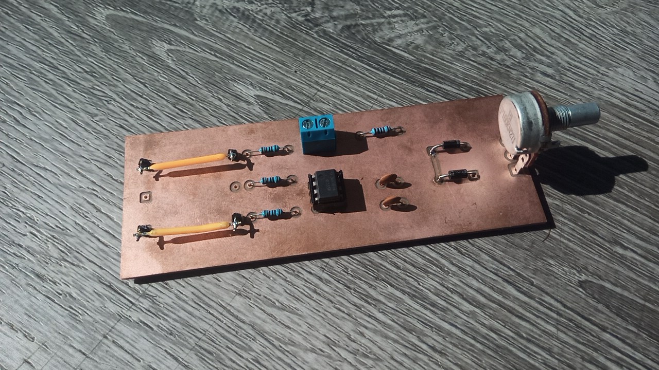
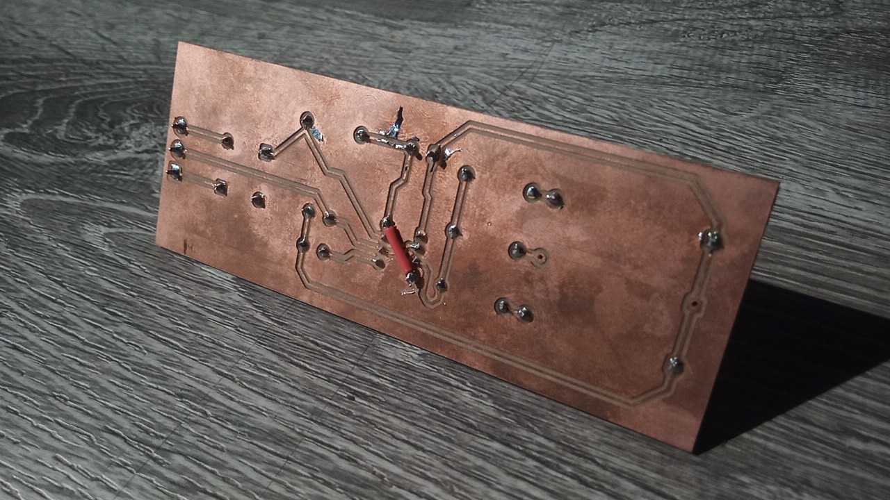
// Front and back of the milled and soldered PCB.
| Milling Tool | Bantam Desktop CNC |
| Board Type | Double-sided FR-1 |
| Design Tool | KiCAD |
| Assembly | Hand soldered |
| Light Source | LED filament module |
| Key Components | NE555, potentiometer, diodes, resistors, capacitors |
Enclosure Design
With a working, tested PCB in hand, the enclosure was designed in OnShape around the board's exact dimensions. The housing integrates the battery holder, potentiometer shaft, switch, and LED filament into a single cylindrical form — I call it the "deodorant stick" lamp. The diffuser was made from transparent PLA filament.
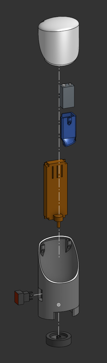
// Exploded assembly view.
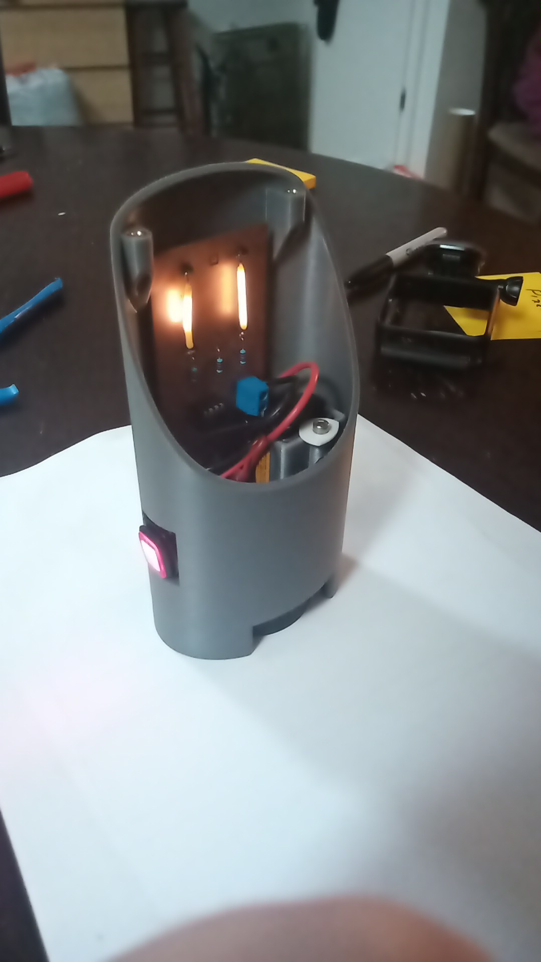
// Assembled lamp during final testing.
Process Summary
Circuit Design & Simulation
NE555 astable PWM circuit designed from reference schematic; validated in Falstad simulation before component selection.
KiCAD Schematic & Layout
Full schematic captured in KiCAD; PCB layout optimized for CNC milling with thru-hole components.
Breadboard Proof-of-Concept
Circuit assembled on breadboard and tested before committing to PCB fabrication.
PCB Mill & Solder
Board milled on Bantam CNC from KiCAD export; components hand-soldered and tested.
Enclosure CAD
Housing designed in OnShape around exact PCB dimensions; diffuser cap, battery pocket, potentiometer routing all integrated.
Print & Final Assembly
Enclosure printed via FDM; all components assembled and final lamp tested.